Taalas Pioneers Hardwired AI Chips to Boost Inference Speed to 17,000 Tokens per Second
Taalas Challenges AI Hardware Norms with Specialized Silicon
In an era where artificial intelligence powers everything from chatbots to autonomous systems, the reliance on versatile but inefficient graphics processing units (GPUs) has long constrained the scalability of AI deployment. Toronto-based startup Taalas is upending this paradigm by developing hardwired AI chips that embed model architectures directly into silicon, promising to make high-performance inference as ubiquitous and affordable as everyday plastics. Taalas’s approach addresses fundamental limitations in current AI infrastructure, where flexibility comes at the expense of efficiency. By shifting from programmable processors to application-specific integrated circuits (ASICs) tailored for particular models, the company aims to eliminate energy-wasting data movements and unlock unprecedented speeds for real-world AI applications.
Tackling the Memory Wall in AI Processing
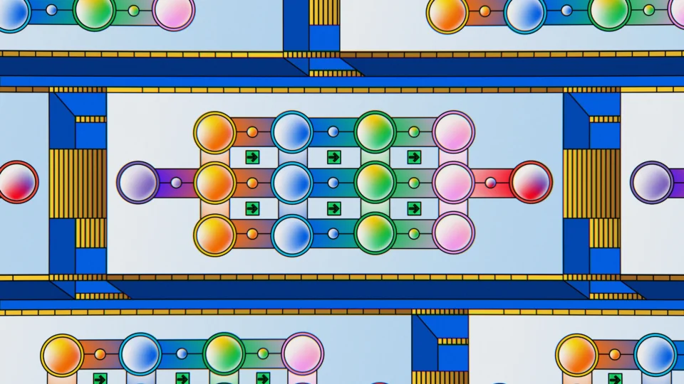
The core challenge in modern AI inference lies in the “memory wall,” a bottleneck where traditional GPUs spend up to 90% of their power shuttling data between high-bandwidth memory (HBM) and processing cores. These instruction set architecture (ISA)-based chips, designed for general-purpose computing, impose a significant “data movement tax” that inflates operational costs in data centers running large language models (LLMs) like Llama 3.1 8B. Taalas counters this with its HC1 (Hardcore 1) chip, which uses a proprietary automated design flow to translate a model’s computational graph— including weights and architecture—directly into the chip’s physical layout. This hardwiring eliminates the need for repeated memory fetches, as the model’s parameters are etched into the silicon’s wiring layers. Still, the HC1 operates without external HBM, relying instead on standard air-cooled systems. Each 250-watt card can be housed in a rack, with up to ten units fitting into a single server to deliver cluster-level performance. This innovation not only reduces power consumption but also simplifies infrastructure, potentially lowering the barriers to deploying AI in resource-constrained environments such as edge devices and industrial sensors.
Achieving Breakthrough Speeds and Efficiency Gains
Taalas’s HC1 chip has demonstrated transformative performance metrics during recent evaluations. When processing the Llama 3.1 8B model, it achieves 16,000 to 17,000 tokens per second—far surpassing the approximately 150 tokens per second of a high-end NVIDIA H100 GPU serving a single user. Key advantages include:
- Performance: A single HC1 outperforms small GPU clusters in raw throughput for targeted models.
- Efficiency: The company reports a 1,000-fold improvement in performance per watt and per dollar, stripping away the overhead of programmability.
- Scalability: Without complex liquid cooling, these chips enable compact, high-density deployments that rival entire GPU setups in a fraction of the space and energy.
To mitigate concerns over model obsolescence, Taalas employs an automated foundry system that generates chip designs from model weights in about one week. By modifying only the top metal masks in the manufacturing process, the full weights-to-silicon turnaround is reduced to roughly two months— a dramatic compression from the traditional two-year, multimillion-dollar ASIC development cycle. This enables a “seasonal” hardware refresh, allowing organizations to deploy customized chips for fine-tuned models within quarters.
Reshaping the AI Market Landscape
Taalas’s advancements signal a broader evolution in the AI ecosystem, transitioning from the research and training phase—dominated by flexible GPUs from NVIDIA and AMD—to a deployment and inference era focused on cost per token. The market could bifurcate into general-purpose training hardware for innovation and specialized inference “foundries” like Taalas, which produce low-cost, model-specific silicon for widespread use. This hardware-defined AI paradigm moves away from software simulations on general-purpose chips toward embedding intelligence natively in devices. Implications extend to societal scales: cheaper, latency-free AI could proliferate in smartphones, sensors, and everyday tools, fostering device-native applications without reliance on cloud subscriptions or centralized servers. As AI inference becomes commoditized, what might this mean for the democratization of intelligence? Could hardwired chips accelerate adoption in underserved sectors, or will they introduce new dependencies on rapid design cycles? The potential for ubiquitous, efficient AI invites reflection on how such shifts could redefine accessibility and innovation in the field.
Fact Check
- Taalas, a Toronto-based startup, develops hardwired AI chips like the HC1 to eliminate memory bottlenecks in inference, achieving up to 17,000 tokens per second on Llama 3.1 8B models.
- Traditional GPUs waste about 90% of energy on data movement, while Taalas claims a 1,000x efficiency gain in performance per watt and dollar with its approach.
- The company’s automated design process shortens chip production from years to two months, focusing on model-specific silicon without high-bandwidth memory needs.
- HC1 chips operate at 250 watts each, supporting air-cooled racks with up to ten units for high-throughput deployments.
- This technology supports a market shift toward specialized inference hardware, complementing general-purpose training tools from NVIDIA and AMD.